페이지 정보
Semiconductor & Display Photo Patternable Materials
Semiconductor & Display Photo Patternable Materials
본문
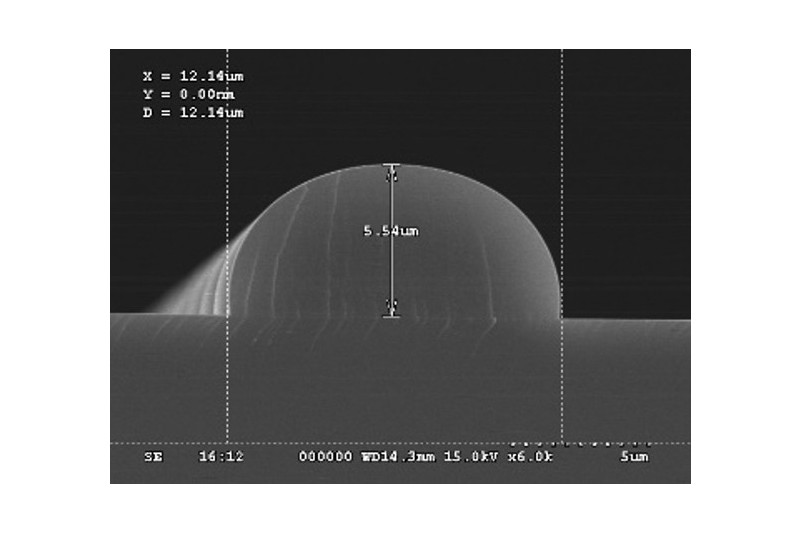
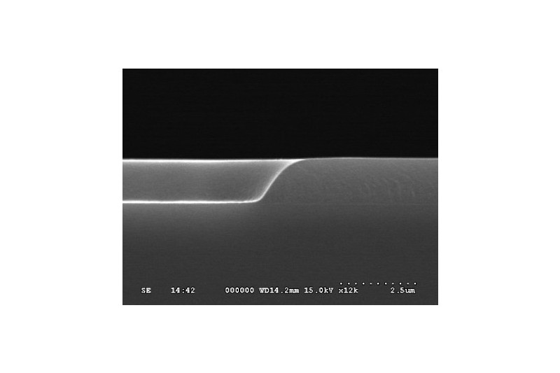
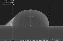
- 실리콘 나노 기술을 이용한 고감도/저유전 Dielectric 개발
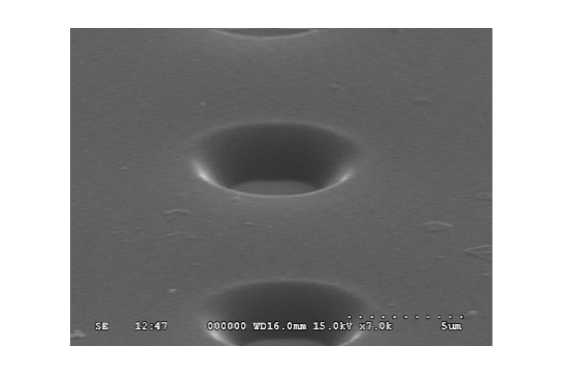
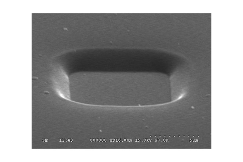
- PHS기술을 이용한 고감도/고해상도 Photo-resist개발
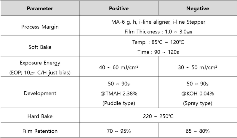
| Type | Key Features |
| Positive | High heat resistance and high resolution through Si polymers and KrF technology |
| Negative | Free from bias and stitch defects through composition technology. |